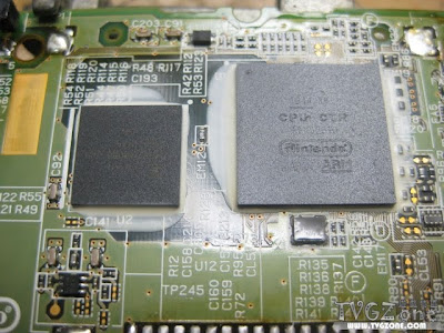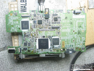
On to the inside, specifically the motherboard itself, and we can see two distinct pieces of silicon that stand out. The first appears to be a single package containing both ARM CPUs, and one DMP PICA200 GPU. Initial impressions seem to hint that it is a SoC (system-on-a-chip) with the individual components most likely all on one die.
The other, is what looks like a block of memory – possibly the entire 96MB that the system is supposed to have – unified as one single pool, from which, due to the overall hardware configuration, it looks like both the CPU and GPU can use. Markings on the chip indicate that it is FCRAM made by Fujitsu, possible a custom solution just for the 3DS as the company doesn’t make FCRAM chips higher than 64Mb.
The use of a unified memory pool is also interesting. Usually this can be limiting for the system if the GPU cannot access it directly. However, from what is known about the main memory and CPU/GPU configuration at the moment, all things point to this not being the case.
In addition to the main 96MB of memory, sources indicated that the 3DS also contains a separate pool of VRAM dedicated to the GPU (rumoured to be around 4MB), which is believed to be located on the SoC. This is most likely to be fast access eDRAM, used just to hold the framebuffer, with the GPU being able to directly access the system’s main memory pool for other things as and when it needs.

From what we can see, the use of a SoC and a separate large block of memory clearly showcases Nintendo’s cost-centric approach when designing the internals of the 3DS. It also looks like being a tidy, efficient set-up. Having all the main components on two separate packages (well the memory appears to be a single chip) keeps cost down, seeing as there is less in the way of overall silicon being used.
It will be interesting to find out just what process node both chips are on. Usually having individual parts groped together on single dies indicates a low process node in the first place, meaning that cooling and heat dissipation should be easy to achieve. In other words, Nintendo have carefully chosen components that not only provide the best ‘bang for your buck’ where the cost/power ratio is concerned, but also ones that should be easy to make future savings on for later revisions of the hardware.
Hopefully, we should find out more shortly after the 3DS’ Japanese launch, when someone else performs a slightly more in-depth teardown of the system, thus allowing us to get a better look at those two chips and the internal hardware make-up as a whole.

No comments:
Post a Comment